


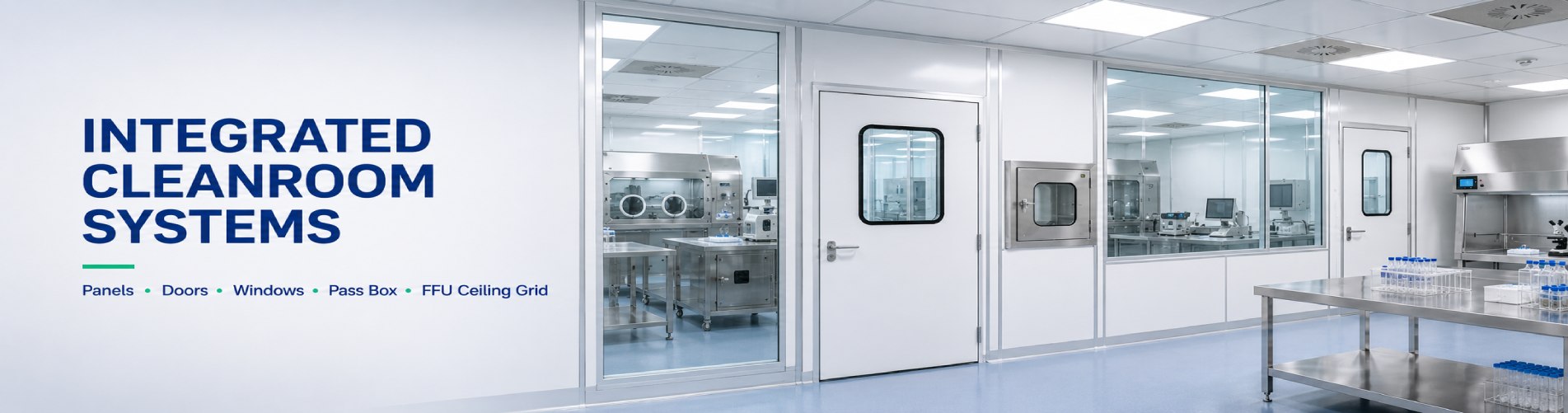


Semiconductor manufacturing is the most demanding contamination-control discipline in industry. The features printed on a modern wafer are measured in nanometres, so a particle far too small to see — well under a micron — can bridge a circuit and ruin a die. Keeping those particles away from the process is not a single filter or product; it is an entire building engineered as a contamination-control system: classified air, unidirectional flow, controlled surfaces, stable temperature and humidity, electrostatic control and vibration isolation, all working together.
This briefing walks through the core elements of a semiconductor cleanroom — what the cleanliness classes actually mean, how the airflow and floor are engineered, what matters beyond particle count, and why a growing share of fab and fab-support space is built from prefabricated, modular components.
01 — Cleanliness classes
What the ISO numbers actually mean
Cleanrooms are classified under ISO 14644-1, which caps the allowed concentration of airborne particles at given sizes. The scale runs from ISO Class 1 (the cleanest) to ISO Class 9 (close to ordinary room air), and each step up allows roughly ten times more particles than the one below it.
Semiconductor work lives at the strict end of that scale. Wafer fabrication and photolithography areas are typically ISO Class 1–5, while less critical assembly, test and packaging spaces may sit at ISO Class 6–8. The decisive detail is that a class is always defined at a particle size: a fab cleanroom is concerned with particles down to 0.1 µm and smaller, because that is the scale at which contamination interacts with today's device geometries.
Particles are not the only enemy. Advanced processes are also sensitive to airborne molecular contamination (AMC) — trace gases and chemical vapours such as acids, bases and organics that can corrode surfaces or disturb lithography long before they would matter in any other setting. A complete strategy therefore pairs particle filtration with chemical filtration and careful material selection, and verifies the result against the target cleanroom classification on handover.
02 — Airflow
Unidirectional airflow: the engine of a fab cleanroom
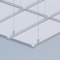
The defining feature of a high-grade semiconductor cleanroom is vertical unidirectional airflow — often called laminar flow. Filtered air is delivered across the whole ceiling and moves straight down through the room in a smooth, even sweep, carrying any particle shed by people, tools or processes downward and out before it can settle on a wafer.
Producing that flow takes two engineered surfaces working as a pair:
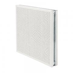
- A fan-filter-unit (FFU) ceiling. The ceiling is filled with FFUs — self-contained modules that each combine a fan with a HEPA or, for the cleanest rooms, a ULPA filter. ULPA media captures an even higher fraction of the finest particles than HEPA, which is why it appears in the most critical fab spaces. The share of ceiling covered by filters (the FFU coverage ratio) rises with the cleanliness class; an ISO Class 5 room can approach full coverage.
- A perforated raised access floor. The work level sits on raised perforated panels. Air drawn down through the room passes through the floor into a plenum below, then returns up the chase to be re-filtered and re-circulated. The open area of the floor tiles is tuned to keep the downward flow even across the whole room.
This ceiling-to-floor loop runs continuously at a high air-change rate, so the room's entire air volume is cleaned many times every hour. At scale, two layouts organise it: the open "ballroom," where one large unidirectional-flow space is shared by many tools, and "bay-and-chase," where clean process bays alternate with service chases that carry return air and utilities.
Vertical unidirectional airflow — ceiling to raised floor
Filtered supply moves straight down; the perforated floor returns it through a plenum for re-filtration.
03 — Beyond clean air
The parameters held in parallel with particle count
Particle control is necessary but not sufficient. Several other variables have to be held inside tight limits at the same time.

Electrostatic discharge (ESD)
Static charge both attracts particles and can damage sensitive devices outright. Semiconductor cleanrooms control it with conductive or dissipative raised floors bonded to ground, dissipative surfaces and footwear, and air ionisation where needed. The green grounding leads visible in many fab rooms are part of this system.
Temperature, humidity, vibration
Photolithography in particular needs tightly held temperature and relative humidity — not for comfort, but because dimensional accuracy, photoresist behaviour and static all depend on them. The HVAC system is sized to hold these within narrow tolerances around the clock. Metrology tools and steppers are also sensitive to vibration, so floors and equipment supports are engineered to isolate it.
Minienvironments, surfaces and monitoring
Rather than hold an enormous room at the very highest class, modern fabs concentrate the cleanest air immediately around the wafer. Tools carry minienvironments, and wafers travel between them in sealed pods (FOUPs) through standardised load ports — so the surrounding room can run a slightly relaxed class and save energy without exposing the wafer. Every interior surface is chosen to shed nothing and outgas as little as possible: flush, sealed wall and ceiling panels with no particle-trapping ledges, coved junctions for cleaning, and low-outgassing finishes. Throughout operation, conditions are tracked by continuous environmental monitoring of particle counts, temperature, humidity and room-to-room pressure, so any drift is caught early.

04 — Construction
Why prefabricated construction increasingly fits the fab
Historically the very largest wafer fabs were built as fixed, stick-built megastructures, and the biggest still are. But a growing share of semiconductor cleanroom space — metrology and inspection rooms, R&D and pilot lines, advanced-packaging and test areas, sub-fab support, and capacity added alongside running production — is built from prefabricated, modular components.
The reasons are practical. Prefabricated panels, FFU ceiling grids, doors and floors are manufactured and quality-checked off site, so the dusty cutting and finishing happens in a factory rather than inside the future clean space. On-site assembly is faster and cleaner, capacity comes online sooner, and — because the envelope bolts together from standard modules — a room can later be reconfigured or expanded as process nodes and tool sets change, without demolishing a validated environment.
The engineering need not compromise to gain that flexibility. In one precision-electronics project at Kunshan Mengxian Electronic Technology, a modular cleanroom was built with top-supply, bottom-return unidirectional airflow, anti-static raised perforated flooring and fully flush enclosures — the same contamination-control principles described above, delivered in prefabricated form. The FFU ceiling grid in such systems is typically extruded in aluminium alloy (6063-T5) so the fan-filter units and ceiling form one engineered, sealed plane. Envelopes built the same way have also reached ISO Class 5 for a demanding consumer-electronics manufacturer — evidence that prefabrication and the strictest cleanliness classes are not at odds.

Specifying a semiconductor cleanroom — the short version
A sound specification starts from the target ISO class for each space and works outward to the systems that achieve it: vertical unidirectional airflow with an appropriate FFU coverage ratio and HEPA or ULPA filtration; a perforated raised access floor and return plenum sized for even flow; chemical filtration where AMC matters; grounded anti-static flooring and ESD controls; tightly held temperature and humidity; vibration isolation for metrology; minienvironments to focus the cleanest air on the wafer; flush, low-outgassing surfaces; and continuous monitoring to prove control. Get those right, and the construction method — stick-built or modular — becomes a question of speed, flexibility and cost rather than of capability.
FAQ
Frequently asked questions
What ISO class does a semiconductor cleanroom need?
Why do semiconductor cleanrooms use vertical unidirectional (laminar) airflow?
What is the difference between HEPA and ULPA filters?
Can prefabricated modular cleanrooms meet semiconductor requirements?
Technical descriptions are simplified for orientation; the correct design and cleanliness target for any facility must be confirmed by a qualified cleanroom engineer.